
To put it as simple as possible, there isn’t really a “right” way to place all the components on your printed circuit board, which means that you can entirely get creative with the design and layout. However, this doesn’t exactly mean that you can do whatever you want with the layout, instead there are some tips that you should follow, especially if you’re a beginner. Fortunately, the article below will feature some of the most important tips that you should follow, including:
1. The Program Needs to Be Suitable
If there is one thing that you should take away from this article, it’s the fact that you must choose a suitable design program that’ll fit all your layout requirements. The program that you choose to use should feature all of the essential features of the PCBs, and by opting for the right one, you can guarantee that you don’t waste your resources. Additionally, as a beginner, you might want to choose something that has a simple platform and that’s easy to navigate.
2. Don’t Choose 90º Trace Angles
One of the most common mistakes most beginners make is choosing trace angles that are higher than 90º. Why is this a mistake? Well, it could generate acid traps, which will in return damage the PCB completely. Instead, you should opt for 45º trace angles since they won’t impact the width of the trace. Keep in mind, narrow angles could easily cause copper migration, which is why you should avoid using them.
3. Don’t Neglect The Final Housing
When you’re outlining the PCB, it’s important to keep the final housing in mind. In most cases, the boards are designed while the housing is still not decided upon, however, in the end, it’ll need it. Hence, you should continue mounting the holes and you should opt for the simple and available housing that will be suitable for the board you’re working on. This can also ensure that the housing gets approved, later on, meaning that you won’t need to do everything again.
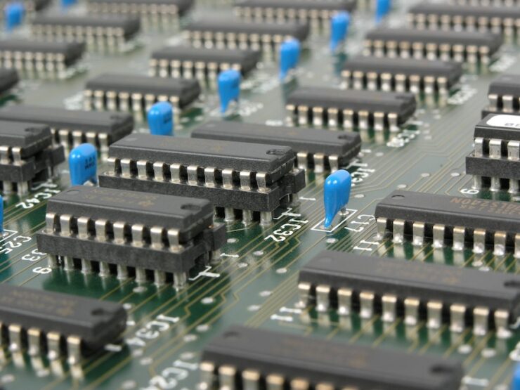
4. There Needs to Be Enough Space Between The Traces
The minimum width between the traces won’t be enough if the board traces need to sustain more than 500mA. After all, the trace on the outside could carry more than an internal trace, mostly because the external one has beet thermal dissipation. The width will heavily rely on how much copper you’ll use and most PCB manufacturers such as uetpcba.com will allow you to opt for different copper weights that range from 0.5 to 2.5 oz/sq.ft.
5. Always Inspect it When You’re Finished
Once you’re done with your PCB layout, you should thoroughly inspect it. Why should you do this? Well, by doing so, you can determine whether or not there are some defects like missing parts, damaged pads, as well as overlapping power traces. This will also guarantee that your printed circuit boards function properly, but more importantly, you can make sure that you don’t have to redesign them later on.
Conclusion
If you just started designing printed circuit boards, the aforementioned tips are some of the most crucial things that you should remember. By doing so, you can guarantee that you don’t waste your resources and time, but more importantly, you could ensure that your PCBs function properly. So, now that you know what you should do, you shouldn’t lose any more time, instead, you should start with the first tip we mentioned – which is choosing a suitable design program.